Creating Cross-Board Nets
A cross-board net is a single net whose endpoints sit on different sub-board PCBs. You declare them on the MBS by wiring module-block pins together, and a sync pushes the cross-board nets out to all the sub-boards.
Refresh from sub-projects
When you change a connector in a sub-project schematic (add pins, rename, remove a Connector symbol), the MBS needs to re-read the sub-projects to stay in sync.
Tools → Refresh from Sub-Projects or the Refresh Module-Blocks button in the tool bar scans every sub-project and presents a diff dialog:
- Blocks added or removed (for new or deleted Connector symbols)
- Pins added, removed, or renamed on existing blocks
- Sub-project paths or UUIDs to update
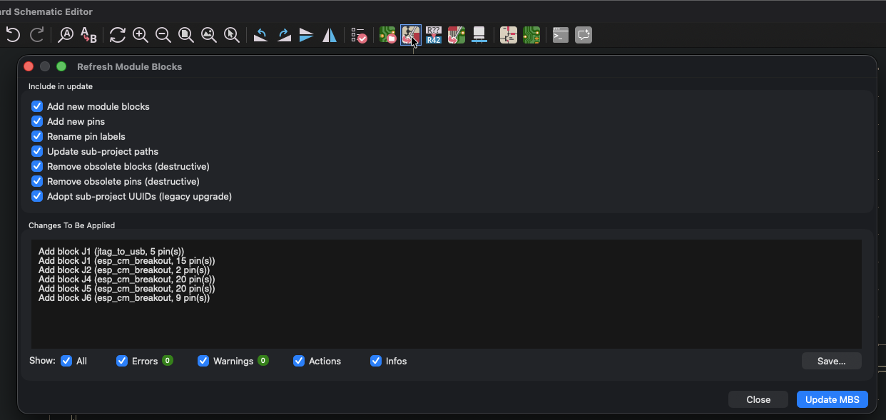
Apply the full diff or check off individual changes. The MBS canvas updates in place; existing wires and cross-board net labels are preserved wherever the underlying pins still exist.
Wiring cross-board nets
Drop a wire between two module-block pins on the MBS. Optionally label it (e.g. USB_DP). That wire defines a connection from the first board's connector pad to the second board's.
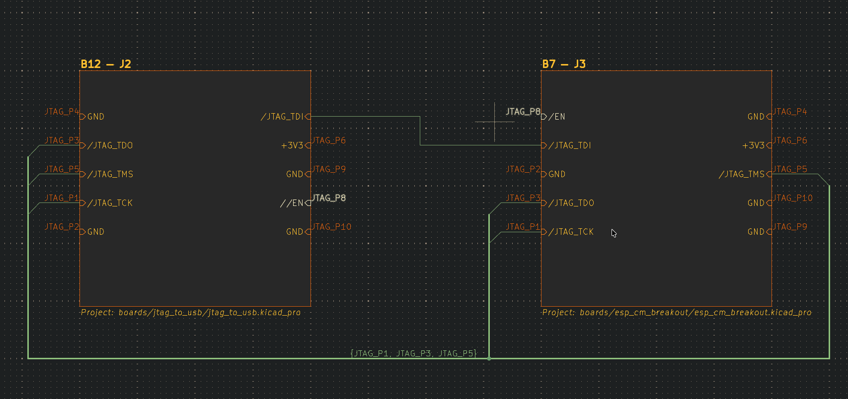
When the MBS is saved, Zeo extracts every connected component on the sheet and writes each one into the container .kicad_pro as a cross-board net with:
- A canonical name (your label, or auto-generated)
- A list of endpoints, one per sub-project, identifying the
(component_ref, pin_number)of the connector pad
Save and sync
File → Save (or Cmd/Ctrl+S) writes the .kicad_mbs to disk and re-extracts every connected component on the active sheet, writing the resulting cross-board net definitions into the container .kicad_pro. The container is the source of truth: Sync to PCB reads cross-board nets from the container, not from the MBS canvas. Save before you sync.
From the MBSCH editor, click the Sync to PCB toolbar button or run Tools → Sync Cross-Board Nets to PCBs. A preview dialog opens with a dry-run pass and no disk writes. The report groups changes per sub-board with severity markers:
- INFO: pad assignments that will be made.
- WARNING: bulk net renames, with the occurrence count for the name being replaced.
- WARNING: naming conflicts when two sub-projects disagree on a local name. The alphabetically-first name wins.
- ERROR: missing footprints or pads that block the sync.
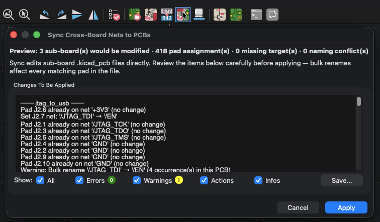
Review the report, then click Apply to commit. The live sync writes to each sub-project's .kicad_pcb on disk (sub-projects don't need to be open; open editors pick up the change on next reload). After apply the dialog stays open with the log visible and Apply morphs to Close. Click Close without Apply to abort without changes.
A net rename is global on the affected PCB: the local name is replaced everywhere it appears in the file, not just on the connector pad. The occurrence count in the preview lets you confirm the scope before committing.
After save and sync, every sub-board PCB carries the cross-board net name on its connector pads. Selecting a cross-board net in any open editor highlights it across every peer board. The container's net classes and cross-board rules apply to it.
Nets you don't wire on the MBS stay local to their sub-board.
From the agent
The same actions are available from the agent as mbs_refresh, mbs_save, and mbs_sync_to_pcb. From Python: refresh_from_sub_projects and sync_to_pcb.